- 您现在的位置:买卖IC网 > Sheet目录486 > NTD110N02RT4 (ON Semiconductor)MOSFET N-CH 24V 12.5A DPAK
�� �
�
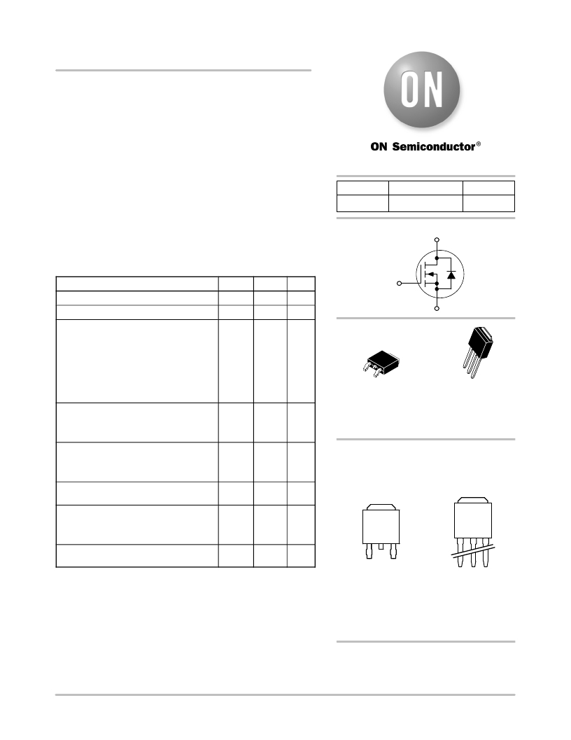
�NTD110N02R, STD110N02R�
�Power� MOSFET�
�24� V,� 110� A,� N� ?� Channel� DPAK�
�Features�
�?� Planar� HD3e� Process� for� Fast� Switching� Performance�
�?� Low� R� DS(on)� to� Minimize� Conduction� Loss�
�?� Low� C� iss� to� Minimize� Driver� Loss�
�?� Low� Gate� Charge�
�?� Optimized� for� High� Side� Switching� Requirements� in�
�High� ?� Efficiency� DC� ?� DC� Converters�
�?� AEC� Q101� Qualified� ?� STD110N02R�
�?� These� Devices� are� Pb� ?� Free� and� are� RoHS� Compliant�
�V� (BR)DSS�
�24� V�
�http://onsemi.com�
�R� DS(on)� TYP�
�4.1� m� W� @� 10� V�
�N� ?� Channel�
�D�
�I� D� MAX�
�110� A�
�MAXIMUM� RATINGS� (T� J� =� 25� °� C� unless� otherwise� noted)�
�Rating�
�Drain� ?� to� ?� Source� Voltage�
�Gate� ?� to� ?� Source� Voltage� ?� Continuous�
�Symbol�
�V� DSS�
�V� GS�
�Value�
�24�
�±� 20�
�Unit�
�V�
�V�
�G�
�S�
�3�
�Thermal� Resistance� ?� Junction� ?� to� ?� Case�
�Total� Power� Dissipation� @� T� C� =� 25� °� C�
�Drain� Current�
�?� Continuous� @� T� C� =� 25� °� C,� Chip�
�?� Continuous� @� T� C� =� 25� °� C�
�Limited� by� Package�
�?� Continuous� @� T� A� =� 25� °� C�
�Limited� by� Wires�
�?� Single� Pulse� (t� p� =� 10� m� s)�
�R� q� JC�
�P� D�
�I� D�
�I� D�
�I� D�
�I� D�
�1.35�
�110�
�110�
�110�
�32�
�110�
�°� C/W�
�W�
�A�
�A�
�A�
�A�
�4�
�1� 2�
�3�
�CASE� 369AA�
�1�
�2�
�CASE� 369D�
�4�
�Thermal� Resistance�
�?� Junction� ?� to� ?� Ambient� (Note� 1)�
�?� Total� Power� Dissipation� @� T� A� =� 25� °� C�
�?� Drain� Current� ?� Continuous� @� T� A� =� 25� °� C�
�R� q� JA�
�P� D�
�I� D�
�52�
�2.88�
�17.5�
�°� C/W�
�W�
�A�
�DPAK�
�(Surface� Mount)�
�STYLE� 2�
�DPAK�
�(Straight� Lead)�
�STYLE� 2�
�4�
�Drain�
�Thermal� Resistance�
�?� Junction� ?� to� ?� Ambient� (Note� 2)�
�?� Total� Power� Dissipation� @� T� A� =� 25� °� C�
�?� Drain� Current� ?� Continuous� @� T� A� =� 25� °� C�
�Operating� and� Storage� Temperature� Range�
�Single� Pulse� Drain� ?� to� ?� Source� Avalanche�
�Energy� ?� Starting� T� J� =� 25� °� C�
�(V� DD� =� 50� Vdc,� V� GS� =� 10� Vdc,�
�I� L� =� 15.5� Apk,� L� =� 1.0� mH,� R� G� =� 25� W� )�
�R� q� JA�
�P� D�
�I� D�
�T� J� ,� T� stg�
�E� AS�
�100�
�1.5�
�12.5�
�?� 55� to�
�175�
�120�
�°� C/W�
�W�
�A�
�°� C�
�mJ�
�MARKING� DIAGRAM�
�&� PIN� ASSIGNMENTS�
�4�
�Drain�
�3�
�Source�
�Maximum� Lead� Temperature� for� Soldering� T� L� 260� °� C�
�Purposes,� (1/8� ″� from� case� for� 10� s)�
�Stresses� exceeding� Maximum� Ratings� may� damage� the� device.� Maximum�
�Ratings� are� stress� ratings� only.� Functional� operation� above� the� Recommended�
�Operating� Conditions� is� not� implied.� Extended� exposure� to� stresses� above� the�
�Recommended� Operating� Conditions� may� affect� device� reliability.�
�1.� When� surface� mounted� to� an� FR4� board� using� 0.5� sq� in� drain� pad� size.�
�2.� When� surface� mounted� to� an� FR4� board� using� the� minimum� recommended�
�pad� size.�
�1�
�Gate�
�2�
�Drain�
�Y� =� Year�
�WW� =� Work� Week�
�T110N2� =� Device� Code�
�G� =� Pb� ?� Free� Package�
�1� 2� 3�
�Gate� Drain� Source�
�ORDERING� INFORMATION�
�See� detailed� ordering� and� shipping� information� in� the� package�
�dimensions� section� on� page� 5� of� this� data� sheet.�
�?� Semiconductor� Components� Industries,� LLC,� 2011�
�August,� 2011� ?� Rev.� 10�
�1�
�Publication� Order� Number:�
�NTD110N02R/D�
�发布紧急采购,3分钟左右您将得到回复。
相关PDF资料
NTD12N10T4
MOSFET N-CH 100V 12A DPAK
NTD14N03RG
MOSFET N-CH 25V 2.5A DPAK
NTD15N06-001
MOSFET N-CH 60V 15A IPAK
NTD15N06L-001
MOSFET N-CH 60V 15A IPAK
NTD18N06L-001
MOSFET N-CH 60V 18A IPAK
NTD18N06T4G
MOSFET N-CH 60V 18A DPAK
NTD20N03L27-001
MOSFET N-CH 30V 20A IPAK
NTD20N06-001
MOSFET N-CH 60V 20A IPAK
相关代理商/技术参数
NTD110N02RT4G
功能描述:MOSFET 24V 110A N-Channel RoHS:否 制造商:STMicroelectronics 晶体管极性:N-Channel 汲极/源极击穿电压:650 V 闸/源击穿电压:25 V 漏极连续电流:130 A 电阻汲极/源极 RDS(导通):0.014 Ohms 配置:Single 最大工作温度: 安装风格:Through Hole 封装 / 箱体:Max247 封装:Tube
NTD12
制造商:OTAX Corporation 功能描述:Tape & Reel
NTD12N06L
制造商:ON Semiconductor 功能描述:
NTD12N08/D
制造商:未知厂家 制造商全称:未知厂家 功能描述:80 V Power MOSFET
NTD12N10
功能描述:MOSFET 100V 12A N-Channel RoHS:否 制造商:STMicroelectronics 晶体管极性:N-Channel 汲极/源极击穿电压:650 V 闸/源击穿电压:25 V 漏极连续电流:130 A 电阻汲极/源极 RDS(导通):0.014 Ohms 配置:Single 最大工作温度: 安装风格:Through Hole 封装 / 箱体:Max247 封装:Tube
NTD12N10-001
功能描述:MOSFET 100V 12A N-Channel RoHS:否 制造商:STMicroelectronics 晶体管极性:N-Channel 汲极/源极击穿电压:650 V 闸/源击穿电压:25 V 漏极连续电流:130 A 电阻汲极/源极 RDS(导通):0.014 Ohms 配置:Single 最大工作温度: 安装风格:Through Hole 封装 / 箱体:Max247 封装:Tube
NTD12N10-1
制造商:ONSEMI 制造商全称:ON Semiconductor 功能描述:Power MOSFET 12 Amps, 100 Volts N−Channel Enhancement−Mode DPAK
NTD12N10-1G
功能描述:MOSFET 100V 12A N-Channel RoHS:否 制造商:STMicroelectronics 晶体管极性:N-Channel 汲极/源极击穿电压:650 V 闸/源击穿电压:25 V 漏极连续电流:130 A 电阻汲极/源极 RDS(导通):0.014 Ohms 配置:Single 最大工作温度: 安装风格:Through Hole 封装 / 箱体:Max247 封装:Tube